I've been aching to make my own linear power supply for some time and I even went the distance of procuring most of the essential parts. All I was left with was finding a proven design to base my build on. In my searches I came across a true gem: a design elaborated in the 50s by the Harrison Laboratories. I was able to reproduce it with common parts and tweak with it to eliminate one auxiliary supply. Although I could have gone down the original full-discrete path, that wasn't very practical, as I'll be showing in the remainder of this article. I chose this model not only for its consistent results and reliable function but in particular because there's much to be learned from it.
Features
- Adjustable voltage (down to 0V),
- Adjustable current,
- Low ripple and noise figures: < 10 mVpp,
- Component limited output current and voltage,
- No overshot on power-on.
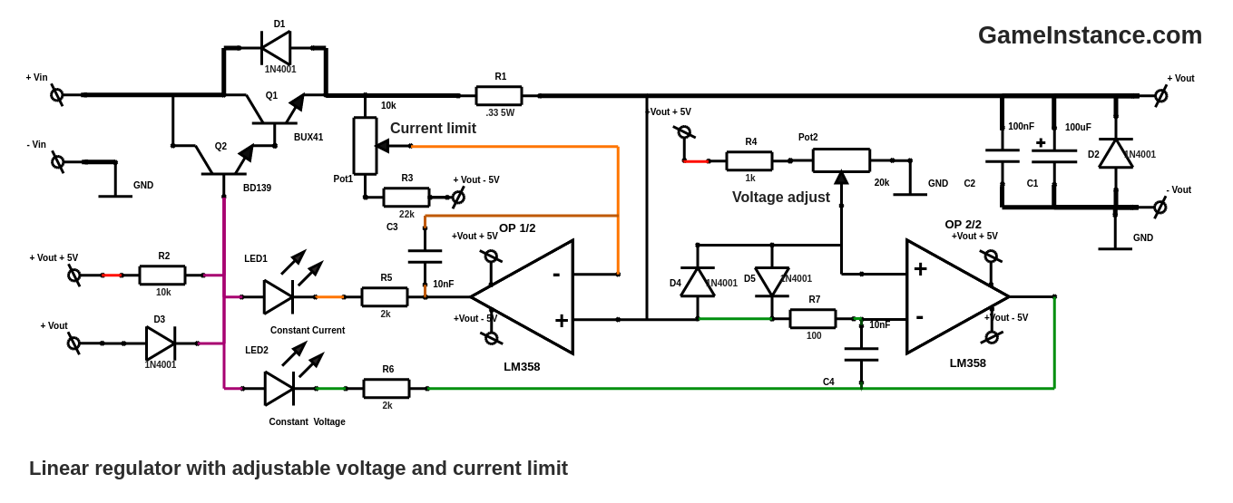
Overview
The circuit takes the input voltage Vin from a rectified and filtered source. Optionally, the source may contain a pre-regulation module having the purpose of reducing the energy dissipated in the series pass transistor Q1.
Vout represents the output voltage and can be used directly or in parallel with an optional crow-bar circuit for over-voltage protection.
Two additional power rails, Vout + 5V and Vout - 5V, are used for polarizing the pass transistor and for powering the op-amps. Both are referenced on the output positive terminal for well founded reasons that will be explained. This in fact is the particularity of the Harrison Labs design.
Regulator and feedback
Q1 is the series pass power transistor and must have a package with a high thermal conductance. That's needed for thermally connecting the silicon to the heat sink element. As a reminder, the transistor may be subjected to high currents and high voltage drops which translates into heat, lots of it. This transistor is polarized by the positive auxiliary power rail through the R2 resistor. If it were not for the rest of the feedback circuit diverting some of that current, Q1 would conduct the maximum rated or available current and provide no regulation. In this example I used a BUX41 mainly because this is the beefiest NPN transistor I have. It could however been any equivalent in TO-3 or TO-220 packages.
The Q1 and Q2 pair forms a Darlington configuration that has the sole purpose of obtaining a higher gain than available for the Q1, which is inherently low with power bipolar transistors. This extra gain allows the use of lower currents to polarize the pass transistor. The lower polarization current has 2 main benefits: the auxiliary supplies can be really low power and the feedback circuit can be low power as well, hence only the use of op-amps. This means that the operation voltage of the polarization line is between 1.2 and 1.4 volts (roughly twice the activation VBE) above the output, not accounting the drop on the current shunt. Considering that the feedback op-amps are themselves powered from two rails that constantly wrap that value, no compromise is made.
The op-amps, OP1/2 and OP2/2, provide the difference amplification and low current driver and are part of the feedback circuit. Basically, any difference between the + and - pins is near-infinitely amplified. Thus, a slight difference between what is and what should be is highlighted and reported to the regulating pass transistor. That applies both for voltage and current.
For the purpose of difference amplification one could use a long-tailed pair, like the one used in the original Harrison design - see the schematic below. It has the same function minus the output amplification. If I would've been fanatic about using discrete components, this is what I would've done.
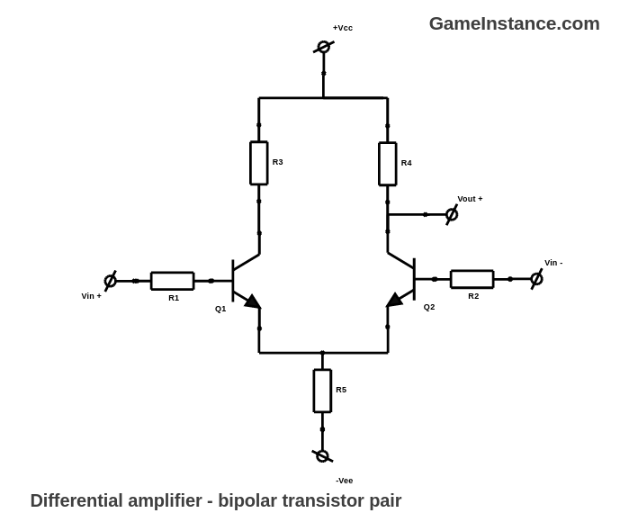
However, there's a problem with this solution. Transistors, even of the same model and from the same production batch, have gain variations that influence the result. If we were to make the effort to match pair transistors, the slightest temperature gradient would cause the same effect. There are matched transistors built in one package that guarantee thermal contact and balanced gains but at that point, the benefits of discrete components are lost and any operational amplifier becomes a better choice. For a device that doesn't necessarily need perfect balancing, this solution would have cut it but the need of 5 carefully chosen resistors just to polarize the transistors would have made the construction less practical.
For the voltage regulating loop, the voltage at the brush of Pot2 must have exactly the same value as the one at the output. If the output voltage were to drop, the reference voltage at the positive input pin of OP2/2 will not drop as fast and will still be able to perform the correction. Observe that the op-amps have no negative feedback and the amplification is near-infinite. The same effect is obtained when the output voltage raises.
Similarly, for the current limiting loop, the voltage at the brush of Pot1 must be exactly the same as the one measured after the current shunt, the R1. If the current were to be higher, the drop on the shunt would rise proportionally giving a lower voltage on the positive input of OP1/2. That would cause op-amp's output to pull towards the negative auxiliary rail, derailing enough current from the Darlington's base current to impose the desired limit.
Bonus features
For both regulating loop circuits, the R5 and R6 resistors have the purpose of limiting the output current and protect the op-amps. The use of Darlington series pass configuration gives a third benefit: the use of LEDs instead of diodes. The low current that needs to be deviated is sufficient to light-up a LED without overloading it. Thus, when the voltage regulator adjusts the output voltage, LED2 is on and LED1 is off. Vice-versa, when the current regulator acts on the output. The purpose of diodes - or LEDs - is to block the op-amps from pushing current into the base of the series pass transistor. The op-amps are allowed only to sink that current.
The capacitors used in the circuit have the purpose of suppressing oscillations. To reiterate, the op-amps have no negative feedback and amplify to their max. Although the transistors in the circuit are fast to react to changes, the propagation times are not negligible causing phase shifts which cause variations that are amplified in a loop. This can be alleviated by adding capacitors at both ends of the amplification circuits - that is the input and output. Moreover, C3 and C4 act as a high frequency negative feedback loop that attenuates fast variations. C1 and C2 form a perfect duo of fast acting and higher capacity buffer for the output voltage, with the same outcome - reducing the inherent tendency of the circuit to oscillate.
There are few diodes in the circuit for protection and limitation purposes. D1 offers a path for currents injected by the DUT (device under test) which could damage the pass transistor. D2 protects the regulator from reverse currents coming from the DUT. Should a problem occur in any of the feedback circuits, D3 limits the polarization voltage from going too much below the Vout level. In normal operation mode, that voltage should be above Vout by at least 1.2V. D4 and D5 keep the voltage regulation differential inputs at one junction drop difference in both directions. This is another protective measure for that op-amp, as it may happen that the set voltage cannot be attained at the output. That kind of protection is unnecessary for the current op-amp as its input voltage difference will never be higher than the drop on the shunt for the known maximum current.
Conclusions
The circuit behaves exemplary, almost unbelievable considering that my breadboard prototype is fed by switch-mode supplies both for Vin and auxiliary rails. It regulates perfectly and has a very low output noise, below 10mV, which is the lowest division my oscilloscope can show. The power transistor can pass 2.5A without problems but if does that on a low impedance consumer, it heats the point that the heat sink cannot manage. This problem can be alleviated with the use of a higher heat sink piece or by using a pre-regulator but this and many others, in a future article.