This is my first notable success in PCB manufacturing. I've made hand-drawn boards before using the permanent marker method but never have I managed to transform a CAD project into a real PCB. This article concentrates around my findings and it won't be detailing all processing steps.
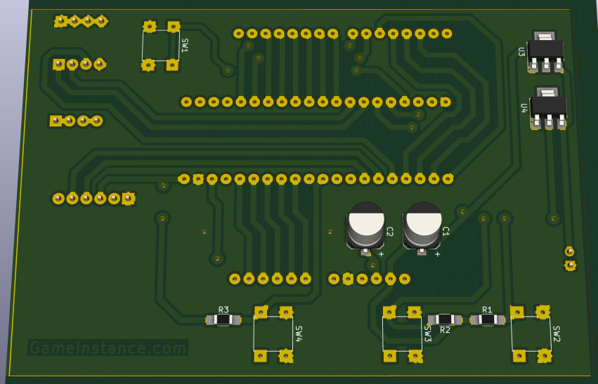 PCB design - a 3D view as rendered by KiCAD's Pcbnew.
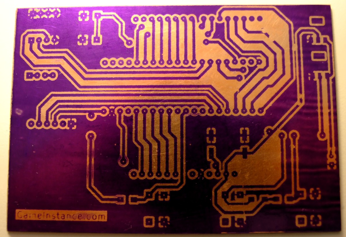
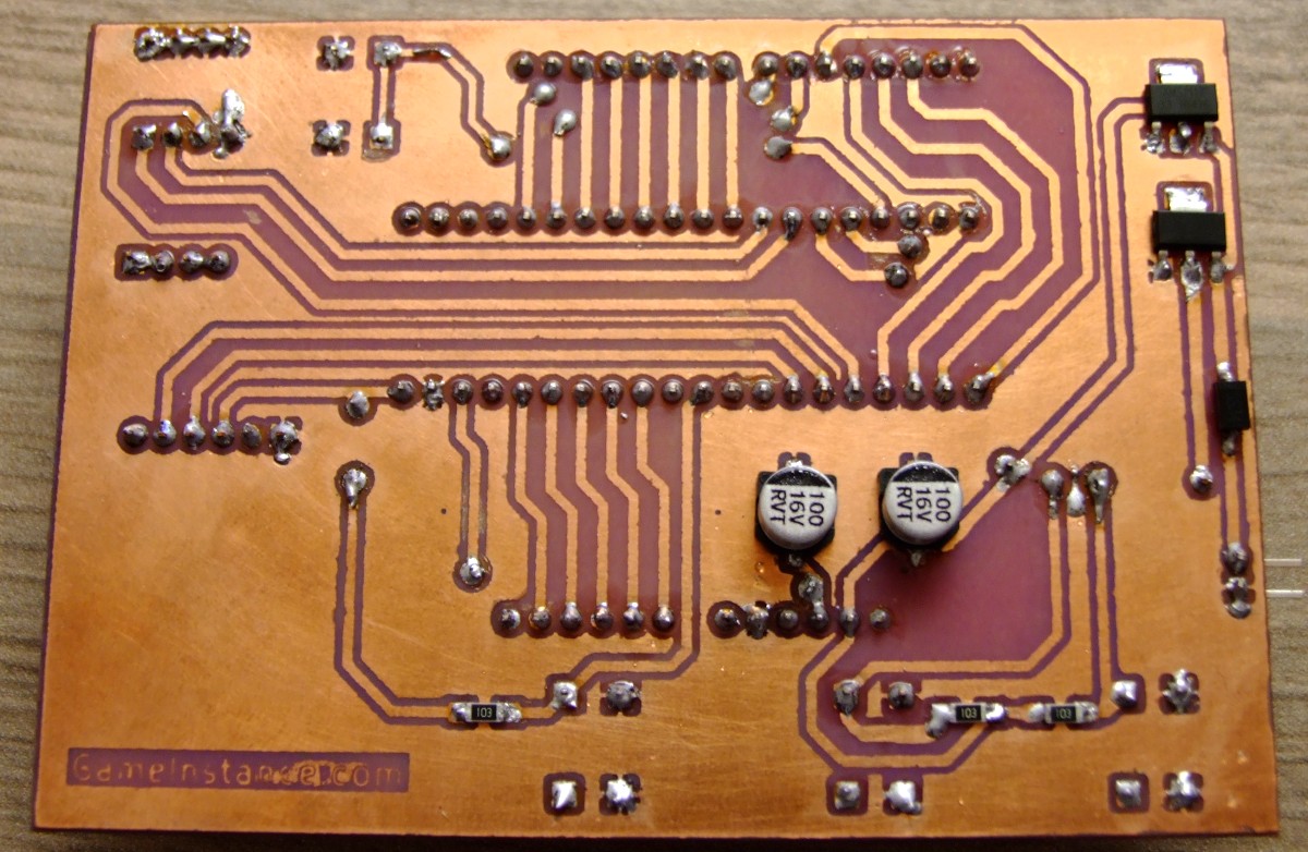 A not-so-great fabricated PCB - the back side, featuring some SMD components.
My conclusions
on the negative UV curable etch mask procedure are the following:
1. Do not expose the film to ambient light. Duh! some would say. Why not? would others. I've read articles from people saying that as long as there's no direct sun light onto the film, it won't change its properties. I have observed the contrary. My negative acting foil has slightly changed its color to a darker blue while handling it in a room with a 40W halogen bulb. There was no direct light hitting the film as I worked behind a shade. The effect is a longer developing of the unexposed regions, with the obvious bad implications. My first application of the foil was to calibrate my UV LED box. I found that it suffices 1 minute of exposure to make the film resistant to a developer of 1/100 concentration. Either my UV box is great - which may not be, considering that I haven't powered the LEDs to the max - or the film is very sensitive. Either way, do not expose the negative photosensitive film to ambient light. I would try the red LEDs solution proposed by Bogdan Raducanu. You'd be able to see what you're doing, reassured that no UV radiation affects your film.
 UV-Box 400 - my hand-built LED UV dual exposure box.
2. Pay special attention to film application. The board needs to be tidy and smooth before applying the sensitive film. That means rubbing it with powder based detergent until every square inch of the board is clean and has a dense network of tiny scratches. Also, uneven board edges will prevent proper clean-up and thus need to be filed-out. The main reason for the excessive care to cleanup is to insure a near perfect adhesion of the film. It may look good when you apply it but if the board has some grease or protective coating on it, the film may go away at the developing step.
3. No ironing. The irony is that the film manufacturers recommend ironing to fix the film on the board. However, I have observed that this does not work. Unless you have a hot press that would apply evenly distributed pressure and controlled heat, the film will form waves towards the middle of the board. The wavy regions will go away first at developing even if they've been hardened in UV light. It suffices a proper clean-up (see point 2 above) and a good hand pressing over the board to remove eventual air bubbles and the film will stick.
4. Extend exposure to the max. The max depends on your setting. In my case the mask was printed on paper and then oiled in sunflower oil - I got the idea from Jari Majaniemi. If 1 minute was enough for a transparent sheet mask, the oily paper required up to 18 minutes of exposure. It seems that the translucent paper blocks a fair amount of UV radiation. For your project you must find the right maximum amount of exposure time without overexposing it. Don't just settle with the first value that works. The more UV radiation hits the photosensitive film, the harder it goes away in the developer. On the same note, I would highly recommend placing the board back in UV light after developing. Of course, this applies for the negative acting films.
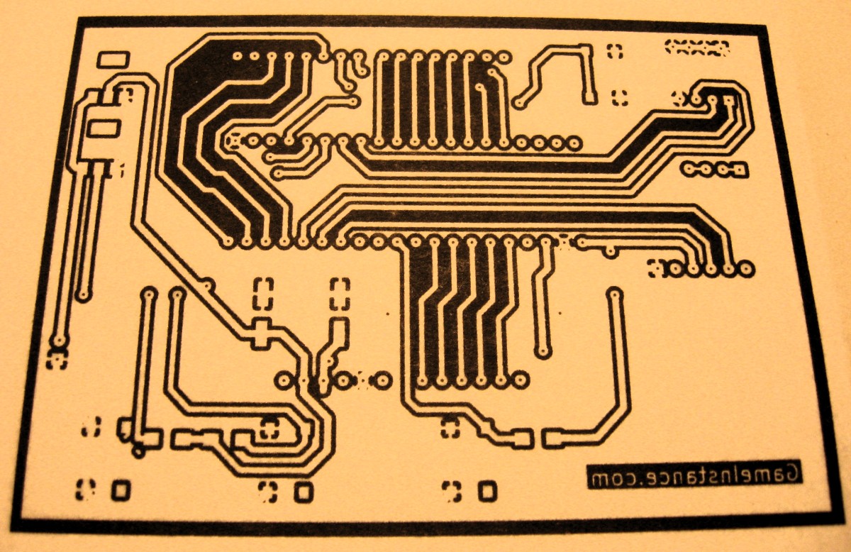 The negative photo mask - a print on regular paper, oiled for translucency.
5. Miscellaneous. It's worth reiterating some other factors that lead to a successful PCB. The mask paper/foil should be pressed onto the board with the printed face forward. This simple thing will minimize transfer errors. Also, it suffices a single oily paper mask to create a good impression. Initially I used 2 sheets to improve the contrast - the black regions were imperfect - but the exposure times were very high, as in half an hour. At the end, the etching process has to be as quick as possible to prevent undermining the thin traces. For this try warming-up the etching solution and agitating it during the process.
 The UV cured positive etch mask. Observable film wavy patterns towards the right-side edge.
The materials
I used standard 10x7 cm single-side copper clad FR-4 boards. They are inexpensive and great for experimenting. Some are a bit rough at the edges - indicating a scissors cut - and need to be filed beforehand. On the board I have applied a negative acting UV curable film. It comes on a plastic roll covered by a black plastic bag. The foil I got had a wavy color pattern towards the edges. I found that those areas turn into an uneven mask after UV curing and that reduced the usable foil surface down to 75%. The developer was an alkaline solution of Sodium Hydroxide. The caustic soda was purchased from the local store in a 25% (at least) concentration solution which made it was a tad safer to work with. I just had to readjust the volumetric proportions. The etching agent was Ferric Chloride bought from an electronics store.
My rant
I find it difficult to work with the photosensitive film and especially applying it properly without leaving fingerprints on the board. There's always one tiny air bubble forming in the middle of the board or a deeper scratch that prevents the adhesion. Those are the trouble regions where the mask won't stick and end-up interrupting traces. Although I have tried ironing with no success, I didn't try heating the board after film application. Given a reasonable temperature, not too high to cook the film, might improve the adhesion. For my future projects I'll be trying presensitized boards or spray photosensitive masks. This will greatly improve the production success rate.
The developing solution I initially used was a bit more concentrated than 1/100. The label on my bottle of sink unclogger indicates having at least 25% caustic soda. I'm sure it hasn't 40% either, but if it's 35% then that's enough to break the concentration limits of my solution. Anyway, I ended-up dripping 0.5 ml of unclogger to 200 ml of water. That gave better results but required a bit more rubbing.
I found useful information about board prepping and etching in a PDF from KontaktChemie.
All my designs are made using KiCAD. It is a free and complete suite that allows the creation of schematics, the edition of pads, footprints and PCB routing. Moreover, it has come a long way in the recent years. It has a rich database of component footprints on GitHub. As a plus, it has an app that enables you to add graphics onto PCBs. Although this is limited to graphical layers, the output file can be altered and your custom drawing may be inserted into copper layers. Having said that, I have a complaint that me and others have verbalized before. The negative image of PCBs can only be exported into PDF, SVG, PS and probably other vectorial formats. Trying to print from a PDF ruins the design and I'm deliberately avoiding the scaling issues. Apparently pads and traces drawn with lines below a certain thickness disappear altogether. I had to use inkscape for editing and printing the PDF/SVG as per Manchester HacSpace, which is a good workaround but still a hack.
The end
This has not turned out exceptionally well. After trashing four boards, I managed to tune my procedure to get a good fifth board. I used thick 1 mm traces just to be on the safe side considering the experimental circumstances. I covered the rest of the surface with the ground power plane to minimize FeCl3 loss. My PCB building is not yet sufficiently refined and there's room for research and experimentation at all fabrication steps.
Keep close for updates on the subject!